Þe "Semiconductor" Section from "Slouching Towards Utopia"
An excerpt from Slouching Towards Utopia <http://bit.ly/3pP3Krk>
I HAVE NOT WRITTEN much in this book about precisely how new technologies have advanced human collective powers over nature, about how they allowed us to organize ourselves in new ways, and what they were and did. I have simply written about their rate of growth: for example, the 2 percent per year in ideas growth after 1870. To have focused on what they were and what they did would have been a very different book, one that needs more of an engineer and less of a political economist. Let me hasten to add that that different book, competently executed, would be a great book about things of vital, perhaps overwhelming, importance. My late teacher David Landes’s Unbound Prometheus accomplished this task for Europe from 1750 to 1965, and it remains a classic. And Robert Gordon has written a new classic covering the United States since 1870 in the same vein.
But right here and now it is, I think, appropriate to bring some features of these technologies to center stage. Consider the idea of General Purpose Technologies (GPTs): those technologies where advances change, if not everything, nearly everything, as they ramify across sector upon sector.5 Steampower in the early 1800s was the first. Early machine tools—embodying in their design and construction so much technological knowledge about how to shape materials—in the mid-1800s were the second. Then after 1870 came telecommunications, materials science, organic chemistry, internal combustion engines, the assembly line, subsequent machine-tool generations, and electricity—the technologies the flowering of which make up Robert Gordon’s “one big wave” of technological advance, and which he sees as transforming the global north over the period 1870–1980 and then ebbing. Starting in the 1950s and reaching critical mass in the 1990s, there came another GPT: microelectronics. Electrons were now made to dance not in the service of providing power but rather to assist and amplify calculation—and communication. And it turned out that microelectronics as microcontrollers could allow the construction of materials that could perform much better and that were cheaper and lighter than relying on dumb matter arranged in ways that linked mechanically.
Take the quartz components of common sand. Purify and liquefy them by heating them to more than 1,700°C (3,100°F). Add carbon to pull the oxygen atoms out of the quartz, leaving behind pure molten liquid silicon. Cool the silicon, and, just before it solidifies, drop a small seed crystal into it. Then pull up the seed crystal and the surrounding silicon attaching itself to it.
If you have done this right, you will then have a monocrystalline silicon cylinder. Slice it finely and thinly into “wafers.” These wafers of pure silicon crystal do not conduct electricity. Why not? Because of a silicon atom’s fourteen electrons, ten cannot move to become currents because they are locked to the nucleus in what chemists call their 1s and 2sp “orbitals.” (“Orbital” is a misnomer: they do not really “orbit.” Niels Bohr a century and more ago thought they did, but he did not have it right. Erwin Schrödinger put him straight.) Only the outermost four electrons, in the 3sp orbitals, might ever get energized and then move around to become electric currents. But in pure silicon they cannot ever do so, because they are locked between their atom’s nucleus and the nuclei of its four neighbors in the crystal. Enough energy to knock them out of the 3sp orbitals and into the “conduction band” orbitals would break the crystal.
But suppose you were to replace a few of the silicon atoms in the crystal—1 in every 10,000 atoms is more than enough—with phosphorus atoms, which have not fourteen but fifteen electrons each. Fourteen of each phosphorus atom’s electrons will act like the silicon atom’s electrons: locked into place, tightly bound in their 1s and 2sp orbitals to their home nucleus, and the outer four bound in their 3sp orbital to both their home nucleus and to the four neighboring nuclei. But the fifteenth electron cannot fit. It finds a higher energy orbital state, in which it is only loosely bound to any one nucleus. It can and does move about in response to small gradients in the local electric field. And so the region of your silicon crystal that you have “doped” with phosphorus becomes a conductor of electricity.
But if you were to do something that pulled those fifteenth electrons away to someplace else, that region would then also become a nonconductive insulator like the rest of the crystal. A doped region of a silicon crystal is thus like the on-off switch on your wall that controls your ceiling light. By applying or removing small voltages of electrical current and electromagnetic pressure, we can flip that switch on and off as we choose, and so let the current flow or not as we choose.
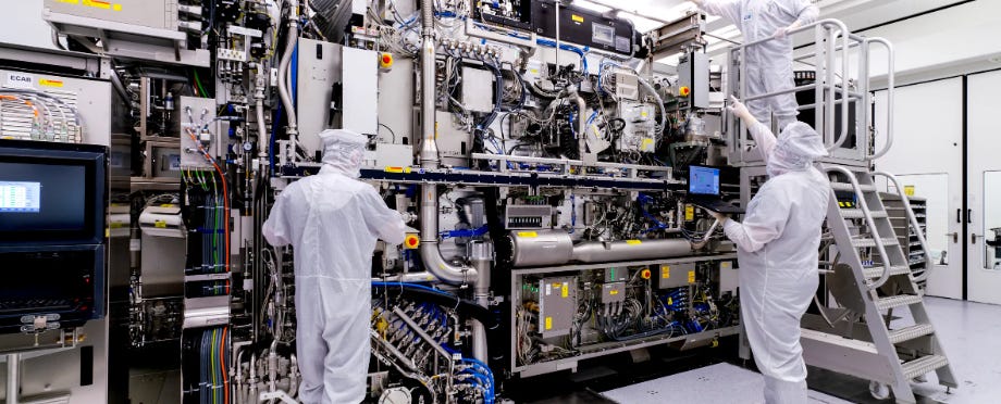
Right now, in the semiconductor fabricators of the Taiwan Semiconductor Manufacturing Company (TSMC), the machines that it has bought (from ASML Holdings in the Netherlands and Applied Materials in Silicon Valley) and installed and programmed are carving 13 billion such semiconductor solid-state switches with attached current and control paths onto a piece of a wafer that will become a crystal silicon “chip” about two-fifths of an inch wide and two-fifths of an inch tall. TSMC’s marketing materials imply that the smallest of the carved features is only twenty-five silicon atoms wide. (In actual fact, the features are more like ten times that size.) If the 13 billion component switches of this small chip of crystal rock made from sand were carved correctly, and it passes its tests, which require that its current pathways switch on and off accurately and synchronously 3.2 billion times a second, the chip will wind up at the heart of a machine like the one connected to the keyboard on which were typed these words. It will be an Apple M1 microprocessor, a very large-scale integrated (VLSI) circuit made up of these tiny switches of doped silicon crystal, which we call transistors.
William Shockley, John Bardeen, and Walter Brattain are the three credited with building the first transistor at Bell Telephone Laboratories in 1947. Dawon Khang and Mohamed Attila are credited with building the first metal-oxide semiconductor field effect transistor. Jay Last’s group, building on the ideas of Robert Noyce and Jean Hoerni of Fairchild Semiconductor, built the first operational solid-state integrated circuit made up of more than one transistor. By 1964 General Microelectronics was making and selling a 120-transistor integrated circuit. Previous vacuum-tube electronic switching elements were 4 inches long—100 millimeters. Transistors in 1964 were packed one-twenty-fifth of an inch, 1 millimeter apart: they were 100 times smaller, enabling 10,000 times as much computation power to be packed into the same space, with orders of magnitude less power consumption.
Gordon Moore, then also working at Fairchild Semiconductor, observed in 1965 that the number of solid-state microelectronic transistors in frontier integrated circuits had grown from 1 to 100 in the seven years since 1958. He made a boldand highly speculative prediction that we could look forward to a future of “component-crammed equipment,” projecting that in 1975, which was just ten years away, a 100 square millimeter silicon chip would hold 65,000 components. That would allow for “electronic techniques more generally available throughout all of society, performing many functions that presently are done inadequately by other techniques or not done at all,” he said. He predicted “home computers—or at least terminals connected to a central computer, automatic controls for automobiles, and personal portable communications.” He said there would be “integrated circuits in digital filters [to] separate channels on multiplex equipment,” and forecast advances in telephone circuits and data processing. “Computers will be more powerful, and will be organized in completely different ways,” he concluded.
By 1971, integrated-circuit semiconductor fabricators had taken four steps downward to a finer process for inscribing patterns on the crystal. The first microprocessor, the Intel 4004, packed 20,000 transistors into a square millimeter—features were 200 microns, 200 millionths of a meter, apart. By 2016 the feature-plus-separation distance was down to 200 nanometers, 200 billionths of a meter. (And by 2021, there would be a further shrinkage, by more than half, and the feature-plus-separation distances would be only 90 nanometers—450 silicon atoms—across).
Back in 1979, to execute 1 MIPS—a million instructions per second—required 1 watt of power. By 2015, 1 watt could drive more than 1 million MIPS. As components became smaller, they became faster. Halve the size of the feature, and you can run it twice as fast—up to a point. Before 1986, microprocessor speed quadrupled every seven years. Then, with the coming of the simplicity of reduced instruction sets, came seventeen years in which each quadrupling of speed took three years rather than seven. Then, after 2003, the quadrupling time went back to seven years, until further speed improvements hit a wall in around 2013.
But the packing of more and more smaller and smaller transistors into VLSI chips continued through what I can only call Deep Magic, albeit at a slower pace than with the original “Moore’s Law.” I can read that the ASML TWINSCAN NXE:3400C machine uses extreme ultraviolet light with a wavelength of 13.5 nanometers, and think: that machine is keeping itself aligned and carving 20 million lines with its lasers into the silicon crystal of a 300 millimeter (12-inch) wafer without erring in positioning any one of those lines by as much as one-thirty-thousandth of a human hair. And I cannot grasp how this could possibly be done, regularly and reliably, for a variable cost of only $50 per microprocessor.
At its most rapid pace during the information-technologyrevolution, the company at the heart of the innovation economy, microprocessor designer and manufacturer Intel, was tick-tocking—tick, improving the microarchitectural details of its micro processors, so programs could run faster; tock, improving the fine resolution of its manufacturing, so that it could make the features, and thus the entire microprocessor, smaller—and completing a full cycle in under three years. With microprocessors doubling in speed every two years, and with the information-technology sector taking full advantage, measured economy-wide productivity growth after 1995 rose again—coming close to its golden-age immediate post–World War II pace—until the Great Recession disruption came at the end of 2007.
The wealth created was spread widely and diffused among users, who gained remarkable capabilities to learn, communicate, and be entertained at an astonishingly low price, and the technoprinces of Silicon Valley and those who assisted them. There were economic disruptions: losers. There were half a million women in the United States staffing telephone switchboards in phone companies and at reception desks in 1960. There are less than two thousand today. But, for the most part, and on the domestic national level for the United States, the coming of information technology to critical mass changed the tasks that had to be done in order to make up the occupation, rather than destroying occupations themselves.
As infotech spread through the economy, the nature of work changed. We East African Plains Apes have long had strong backs and thighs with which to move heavy objects, nimble fingers to do fine work, mouths and ears with which to communicate, and brains with which to think, and manipulate symbols. Starting with the domestication of the horse and continuing with the steam engine, the place of backs and thighs in human work had been greatly reduced by 1870, but there was still plenty of fine manipulation to do. With the coming of electricity and its machinery, human fingers began to be replaced by machines also, but there was still a huge amount of complex design to be done, along with brainstorming and routine accounting and informing, all work to be done by brains, mouths, and ears. Every machine required a microcontroller, and the human brain was by far the best one available.
So technology had so far complemented labor rather than substituting for it: more machines and more information technology made human beings more valuable and more productive, rather than less so. But to many, the new work seemed less like the type of thing that a high-status master craftsman might do and more like the tasks required of a servant—either of the cus- tomer, or of the increasingly autonomous-looking machine itself.
On the international scale, information technology plus on-going reglobalization turned, in the 1990s when infotech reached critical mass, into hyperglobalization.
The international economist Richard Baldwin put his finger on the pulse of what he calls the “second unbundling”: that of intra-firm communication. With the coming of the Internet, it was no longer necessary for a firm’s sophisticated industrial division of labor to be geographically concentrated. You no longer had to be able to walk or drive to your supplier’s offices and factories to show them how what they had was not quite what you needed. You could, first, in the 1980s, draw a picture and send a fax. Then, in the 1990s, you could send an email. By the late 2000s you could send multi-megabyte data files around the globe.
And for those—many—cases in which words-on-paper or words-and-pictures-on-screen were not enough? After 1990, increasingly, you could hop onto an overnight transoceanic non-stop jet. The word is that Apple Computer had fifty first-class seats a day back and forth between San Francisco and China in the months before the coming of the COVID-19 plague. And for those cases in which the limits of the division of labor were not so much the communication of knowledge but the face-to- face, looking-in-the-eye establishment of trust and its limits? The transoceanic airplane flight worked there as well. Thus, after 1990, manufacturing, which had been increasingly concentrating itself in the global north since 1800, began to spread out away from the global north at tremendous speed. Not just better—but revolutionarily and superlatively better—communications made it possible to spread out what had been regional concentrations of firms into globe-spanning value chains.
The extraordinary wage gaps that a century of economic divergence had created between global north and global south made all of this immensely profitable. In the space of a generation, with the spreading-out of production into globe-spanning value-chain networks, much of global manufacturing became both high-tech and low-wage.